|
Electronic Components Datasheet Search |
|
|
Electronic Components Datasheet Search |
|
BS640HD9V Datasheet(PDF) 38 Page - Advanced Micro Devices |
|
|
|||||||||||||||||||||||||||||
BS640HD9V Datasheet(HTML) 38 Page - Advanced Micro Devices |
|
|
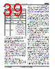
38 / 89 page  36 Am29BDS128H/Am29BDS640H 27024B3 May 10, 2006 D A TA SH EE T Table 18. Configuration Register Note:Device will be in the default state upon power-up or hardware reset. Reset Command Writing the reset command resets the banks to the read or erase-suspend-read mode. Address bits are don’t cares for this command. The reset command may be written between the sequence cycles in an erase command sequence before erasing begins. This resets the bank to which the system was writing to the read mode. Once erasure begins, however, the device ignores reset commands until the operation is complete. The reset command may be written between the sequence cycles in a program command sequence before programming begins (prior to the third cycle). This resets the bank to which the system was writing to the read mode. If the program command sequence is written to a bank that is in the Erase Suspend mode, writing the reset command returns that bank to the erase-suspend-read mode. Once programming begins, however, the device ignores reset commands until the operation is complete. The reset command may be written between the sequence cycles in an autoselect command sequence. Once in the autoselect mode, the reset command must be written to return to the read mode. If a bank entered the autoselect mode while in the Erase Suspend mode, writing the reset command returns that bank to the erase-suspend-read mode. If DQ5 goes high during a program or erase operation, writing the reset command returns the banks to the read mode (or erase-suspend-read mode if that bank was in Erase Suspend). Autoselect Command Sequence The autoselect command sequence allows the host system to access the manufacturer and device codes, and determine whether or not a sector is protected. Table 20, “Memory Array Command Definitions,” on page 46 shows the address and data requirements. The autoselect command sequence may be written to an address within a bank that is either in the read or erase-suspend-read mode. The autoselect command may not be written while the device is actively program- ming or erasing in the other bank. The autoselect command sequence is initiated by first writing two unlock cycles. This is followed by a third write cycle that contains the bank address and the autoselect command. The bank then enters the autoselect mode. No subsequent data will be made available if the autoselect data is read in synchronous mode. The system may read at any address within the same bank any number of times without initiating another autoselect command sequence. Read com- mands to other banks will return data from the array. The following table describes the address require- ments for the various autoselect functions, and the resulting data. BA represents the bank address, and Address BIt Function Settings (Binary) A19 Set Device Read Mode 0 = Synchronous Read (Burst Mode) Enabled 1 = Asynchronous Mode (default) A18 RDY 0 = RDY active one clock cycle before data 1 = RDY active with data (default) A17 Clock 0 = Burst starts and data is output on the falling edge of CLK 1 = Burst starts and data is output on the rising edge of CLK (default) A16 A15 Read Mode Synchronous Mode 00 = Continuous (default) 01 = 8-word linear with wrap around 10 = 16-word linear with wrap around 11 = 32-word linear with wrap around A14 A13 A12 Programmable Wait State 000 = Data is valid on the 2th active CLK edge after AVD# transition to VIH 001 = Data is valid on the 3th active CLK edge after AVD# transition to VIH 010 = Data is valid on the 4th active CLK edge after AVD# transition to VIH 011 = Data is valid on the 5th active CLK edge after AVD# transition to VIH 100 = Data is valid on the 6th active CLK edge after AVD# transition to VIH 101 = Data is valid on the 7th active CLK edge after AVD# transition to VIH (default) 110 = Reserved 111 = Reserved |
|
Link URL |
| Does ALLDATASHEET help your business so far? [ DONATE ] |
About Alldatasheet | Advertisement | Datasheet Upload | Contact us | Privacy Policy | Link to Datasheet | Link Exchange | Manufacturer List All Rights Reserved©Alldatasheet.com |
| Russian : Alldatasheetru.com | Korean : Alldatasheet.co.kr | Spanish : Alldatasheet.es | French : Alldatasheet.fr | Italian : Alldatasheetit.com Portuguese : Alldatasheetpt.com | Polish : Alldatasheet.pl | Vietnamese : Alldatasheet.vn Indian : Alldatasheet.in | Mexican : Alldatasheet.com.mx | British : Alldatasheet.co.uk | New Zealand : Alldatasheet.co.nz |
|
Family Site : ic2ic.com |
icmetro.com |
 English ▼
 English
 Chinese
 German
 Japanese
 Russian
 Korean
 Spanish
 French
 Italian
 Portuguese
 Polish
 Vietnamese
 Indian
 Mexican
 British
 New Zealand