|
Electronic Components Datasheet Search |
|
|
Electronic Components Datasheet Search |
|
EM62100AGH Datasheet(PDF) 14 Page - ELAN Microelectronics Corp |
|
|
|||||||||||||||||||||||||||||
EM62100AGH Datasheet(HTML) 14 Page - ELAN Microelectronics Corp |
|
|
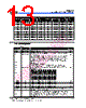
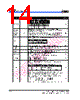
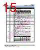
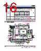
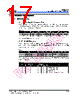
14 / 60 page  EM62100 65 COM/132 SEG STN LCD Driver 8 • ••• Product Specification (V1.1) 09.13.2005 (This specification is subject to change without further notice) Pin Name I/O Function No.ofPins DUTY0 DUTY1 I Select the maximum LCD driver duty DUTY1 DUTY 0 LCD Driver Duty 0 0 1/33 0 1 1/49 1 0 1/55 1 1 1/65 2 D0, D1, D2, D3, D4, D5, D6 (SCL), D7 (SI) I/O 8-bit bi-directional data bus connected to an 8-bit or 16-bit standard MPU data bus. When the chip select is inactive, D0 to D7 are set to high impedance. When serial interface is selected (P/S = “L”), then D7 serves as the serial data input terminal (SI) and D6 serves as the serial clock input terminal (SCL). During this time, D0 to D5 are set to high impedance. 16 Determines whether the data bits are data or instruction (command). RS D0 to D7 H Display data L Instruction (Command) RS I 1 RESB I When RESB is set to “L,” the settings are initialized. 19 CS1B CS2 I Chip select signal. When CS1B = “L” and CS2 = “H,” then the chip select CS2 becomes active, and data/command I/O is enabled. 2 RDB (E) I Enable clock signal input for the 68-series MPU, active high. Active low input pin for the 80-series MPU RDB signal 1 WRB (RW) I Read/Write control signal with 68-series MPU RW=”H”: Read, RW=”L”: Write Active low input pin for the 80 series MPU WRB signal 1 M86 I MPU interface switch terminal M86 =”H”: 68-series MPU interface M86 =”L”: 80-series MPU interface 1 Selects the Parallel or Serial data input interface P/S = “H”: Parallel data input interface, P/S = “L”: Serial data input interface The following applies depending on the P/S status: P/S Data/Command Data Read/Write Serial Clock H RS D0 to D7 RDB (E), WRB (RW) L RS D7 (SI) Write only D6 (SCL) P/S I When P/S = “L”, D0 to D5 are hi-Z. D0 to D5 can be “H” or “L” RDB (E) and WRB (RW) are fixed to either “H” or “L”. With serial data input, RAM display data reading is not supported. 1 CKS I Terminal to select whether enable or disable the display clock internal oscillator circuit. CKS = “H”: Internal oscillator circuit is enabled CKS = “L”: Internal oscillator circuit is disabled (requires an external input) When CKS = “L”, input the display clock through the CK terminal. 1 |
|
Link URL |
| Does ALLDATASHEET help your business so far? [ DONATE ] |
About Alldatasheet | Advertisement | Datasheet Upload | Contact us | Privacy Policy | Link to Datasheet | Link Exchange | Manufacturer List All Rights Reserved©Alldatasheet.com |
| Russian : Alldatasheetru.com | Korean : Alldatasheet.co.kr | Spanish : Alldatasheet.es | French : Alldatasheet.fr | Italian : Alldatasheetit.com Portuguese : Alldatasheetpt.com | Polish : Alldatasheet.pl | Vietnamese : Alldatasheet.vn Indian : Alldatasheet.in | Mexican : Alldatasheet.com.mx | British : Alldatasheet.co.uk | New Zealand : Alldatasheet.co.nz |
|
Family Site : ic2ic.com |
icmetro.com |
 English ▼
 English
 Chinese
 German
 Japanese
 Russian
 Korean
 Spanish
 French
 Italian
 Portuguese
 Polish
 Vietnamese
 Indian
 Mexican
 British
 New Zealand