|
Electronic Components Datasheet Search |
|
|
Electronic Components Datasheet Search |
|
ADG774ABCPZ-R2 Datasheet(PDF) 4 Page - Analog Devices |
|
|
|||||||||||||||||||||||||||||
ADG774ABCPZ-R2 Datasheet(HTML) 4 Page - Analog Devices |
|
|
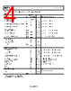
4 / 14 page  ADG774A Data Sheet Rev. C | Page 4 of 14 VDD = 3 V ± 10%, GND = 0 V, all specifications TMIN to TMAX, unless otherwise noted.1 Table 2. B Version Parameter 25°C TMIN to TMAX Unit Test Conditions/Comments ANALOG SWITCH Analog Signal Range 0 to 1.5 V On Resistance, RON 4 Ω typ VD = 0 V to 1 V; IS = −10 mA 6 7 Ω max On Resistance Match Between Channels, ∆RON 0.15 Ω typ VD = 0 V to 1 V, IS = −10 mA 0.5 Ω max On Resistance Flatness, RFLAT(ON) 1.5 Ω typ VD = 0 V to 1 V, IS = −10 mA 3 Ω max LEAKAGE CURRENTS Source Off Leakage, IS (OFF) ±0.001 nA typ VD = 2 V/1 V, VS = 1 V/2 V, see Figure 17 ±0.1 ±0.25 nA max Drain Off Leakage, ID (OFF) ±0.001 nA typ VD = 2 V/1 V, VS = 1 V/2 V, see Figure 17 ±0.1 ±0.25 nA max Channel On Leakage, ID, IS(ON) ±0.001 nA typ VD = VS = 2 V/1 V, see Figure 18 ±0.1 ±0.25 nA max DIGITAL INPUTS Input High Voltage, VINH 2.0 V min Input Low Voltage, VINL 0.4 V max Input Current IINL or IINH 0.001 μA typ VIN = VINL or VINH ±0.1 μA max Digital Input Capacitance, CIN 3 pF typ DYNAMIC CHARACTERISTICS2 tON, tON (EN) 7 ns typ CL = 35 pF, RL = 50 Ω, VS = 1.5 V, see Figure 22 14 ns max tOFF, tOFF (EN) 4 ns typ CL = 35 pF, RL = 50 Ω, VS = 1.5 V, see Figure 22 8 ns max Break-Before-Make Time Delay, tD 3 ns typ CL = 35 pF, RL = 50 Ω, VS1 = VS2 = 1.5 V, see Figure 23 1 ns min Off Isolation −65 dB typ f = 10 MHz, RL = 50 Ω Channel-to-Channel Crosstalk −70 dB typ f = 10 MHz, RL = 50 Ω, see Figure 21 Bandwidth −3 dB 400 MHz typ RL = 50 Ω, see Figure 19 Distortion 1.5 % typ RL = 100 Ω Charge Injection 4 pC typ CL = 1 nF, see Figure 24, VS = 0 V CS (OFF) 5 pF typ CD (OFF) 7.5 pF typ CD, CS (ON) 12 pF typ POWER REQUIREMENTS VDD = 3.3 V Digital inputs = 0 V or VDD IDD 1 μA max 0.001 μA typ 1 Temperature range for B version is −40°C to +85°C. 2 Guaranteed by design, not subject to production test. |
|
|
Link URL |
| Does ALLDATASHEET help your business so far? [ DONATE ] |
About Alldatasheet | Advertisement | Datasheet Upload | Contact us | Privacy Policy | Link to Datasheet | Link Exchange | Manufacturer List All Rights Reserved©Alldatasheet.com |
| Russian : Alldatasheetru.com | Korean : Alldatasheet.co.kr | Spanish : Alldatasheet.es | French : Alldatasheet.fr | Italian : Alldatasheetit.com Portuguese : Alldatasheetpt.com | Polish : Alldatasheet.pl | Vietnamese : Alldatasheet.vn Indian : Alldatasheet.in | Mexican : Alldatasheet.com.mx | British : Alldatasheet.co.uk | New Zealand : Alldatasheet.co.nz |
|
Family Site : ic2ic.com |
icmetro.com |
 English ▼
 English
 Chinese
 German
 Japanese
 Russian
 Korean
 Spanish
 French
 Italian
 Portuguese
 Polish
 Vietnamese
 Indian
 Mexican
 British
 New Zealand